- Retrait gratuit dans votre magasin Club
- 7.000.000 titres dans notre catalogue
- Payer en toute sécurité
- Toujours un magasin près de chez vous
- Retrait gratuit dans votre magasin Club
- 7.000.0000 titres dans notre catalogue
- Payer en toute sécurité
- Toujours un magasin près de chez vous
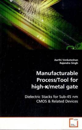
Manufacturable Process/Tool for high-κ/metal gate
Aarthi Venkateshan, Rajendra Singh
Livre broché | Anglais
77,95 €
+ 155 points
Description
Off state leakage current related power dominates the CMOS heat dissipation problem of state of the art silicon integrated circuits. In this study, this issue has been addressed in terms of a low-cost single wafer processing (SWP) technique using a single tool for the fabrication of high-κ dielectric gate stacks for sub-45 nm CMOS. A system for monolayer photoassisted deposition was modified to deposit high-quality HfO2 films with in-situ clean, in-situ oxide film deposition, and in-situ anneal capability. The system was automated with Labview 8.2 for gas/precursor delivery, substrate temperature and UV lamp. The gold-hafnium oxide-aluminum (Au-HfO2-Al) stacks processed in this system had superior quality oxide characteristics with gate leakage current density on the order of 1 x 10-12 A/cm2 @ 1V and maximum capacitance on the order of 75 nF for EOT=0.39 nm. Achieving low leakage current density along with high capacitance demonstrated the excellent performance of the process developed. Detailed study of the deposition characteristics such as linearity, saturation behavior, film thickness and temperature dependence was performed for tight control on process parameters. Using Box-Behnken design of experiments, process optimization was performed for an optimal recipe for HfO2 films. UV treatment with in-situ processing of metal/high-κ dielectric stacks was studied to provide reduced variation in gate leakage current and capacitance. High-resolution transmission electron microscopy (TEM) was performed to calculate the equivalent oxide thickness (EOT) and dielectric constant of the films. Overall, this study shows that the in-situ fabrication of MIS gate stacks allows for lower processing costs, high throughput, and superior device performance.
Spécifications
Parties prenantes
- Auteur(s) :
- Editeur:
Contenu
- Nombre de pages :
- 204
- Langue:
- Anglais
Caractéristiques
- EAN:
- 9783836481564
- Date de parution :
- 06-11-08
- Format:
- Livre broché
- Format numérique:
- Trade paperback (VS)
- Dimensions :
- 152 mm x 229 mm
- Poids :
- 281 g

Les avis
Nous publions uniquement les avis qui respectent les conditions requises. Consultez nos conditions pour les avis.


